Tweaks
Building for Tweakability
It’s possible to use Molex KK series 0.1" connectors for all connections to the PIMETA v2 board. This makes working on your PIMETA after casing it up easier, as you can simply disconnect the board from the enclosure’s panels. Otherwise, you have to desolder connections to work on it, or use hookup wires long enough to allow working on the board while it’s still hooked up to the panels.
There’s explicit support for this with the S1, INPUTS, WALL and BATT connections.
It’s also possible to do this for the volume control with one 3-pin KK in the front set of ALPS RK097 pads and another in the DACT CT2 pads.
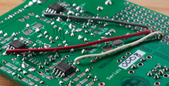
Doing this for the output pads is easy enough by using the scratchpad area, as shown at right. There are many 2-pad pairs in this area. Choose a group of 3 adjacent pairs, run hookup wires from the Ox pads to this group, leaving the other three holes for a 3-pin Molex connector. Although the pin order doesn’t matter, you might consider using the same order as in the INPUTS connector, to avoid confusion. Also, I find it helpful in testing when I use a different wire color for each pin.
You might also consider adding pin sockets for some of the resistors. It’s popular to do this for R4, to allow swapping it for easy tweaking of the gain, and for RLED to allow easy adjustment of LED1’s brightness. Although you can buy individual pin sockets, I keep SIP socket strips in my part bins for other purposes, so I just cut individual pins from one of these, using my wire cutters to break the plastic bits away.
The Scratchpad Area
The PIMETA v2 has a section of patterned perfboard, which we like to call the “scratchpad.” This area is for experimentation, expansion, and customization. It’s fairly small as perfboard goes, but keep in mind that you don’t have to provide your own power supply or other support circuitry. What you couldn’t manage to fit into a lone piece of perfboard this small might be practical as a kind of sidecar to the PIMETA board.
Here are some ideas for ways to use this area:
Third rail cap: If two C2s isn’t enough for you, you can put a 16 or 18 mm diameter cap across the long bus strips in the DIP area, and use the pads connected to it to connect the cap to B+ and V- with hookup wire. Or, you can perhaps use the extra lead length in the cap to make this jump, though I’d use heat shrink to avoid shorts.
Microcontroller madness: There are hundreds of DIP-packaged microcontrollers on the market that will fit here, the largest being a DIP-18. I’m partial to 8-pin PICs, myself; tiny little powerhouses with lots of built-in peripherals. Particular favorites are the PIC12F675 and 683 when I need processing power or a fair bit of code, or the PIC10F220 and 222 when I just need a simple little digital problem-solver.
The possibilities here are vast. Low-voltage supply cut-off? Output DC offset protection? Digital potentiometer control? Web-controlled headphone amp? (lynx pimeta2.myhouse.org) You’ve got more potential power here with a few dollars in parts than we had in an early 80’s microcomputer costing a few thousand dollars.
Op-amps, comparators and buffers, oh my: Microcontrollers aren’t the only 8-pin powerhouses out there:
Battery charge indicator: A comparator and a little bit of external circuitry can drive a bicolor power LED that changes color based on the battery voltage: green for a fresh battery, yellow for one nearly used up, and red for “charge me now!”
Fourth amp channel: There’s room enough here for a complete fourth buffered amplifier channel, allowing you to convert the PIMETA to balanced headphone drive.
Secondary output: Run wires from any of several points in the circuit to a chip that can drive an alternate output connector. The extra active stage will let both connectors be used at once without the one loading the other. Several configurations come to mind:
Combined Headamp and Preamp: Run wires from the extra pot wiper pads to a dual op-amp configured as a buffer, to get a volume-controlled output. Use IG for the connector grounds, not OG, to avoid shorting out the PIMETA’s ground channel through the audio system ground.
Simple Line Out: Same as above, but run the wires from the extra C1 pads, either before or after the cap.
XLR Line Out: Like above, but instead of op-amps, use balanced driver chips. These are specialized, and often larger than op-amps, but there’s room here for two single-channel driver chips.
Balanced receiver: If your source uses balanced audio (XLR plugs) you could put a couple of balanced receivers here, like the INA121, and run their output to the PIMETA’s INPUTS connector.
Supply voltage boost: Imagine using the 2×AA version of the Serpac H-65 case with 2500 mAh NiMH rechargeables along with a little DIP-8 voltage doubler chip, and suitable filtering in the scratchpad area. Doubling the voltage will more than double the current draw from the batteries — can’t go creating free energy — but 1000 mAh or so is still pretty attractive. You’ll have to be choosy about your op-amps to get something that will run from 5-6 V, but there are several popular ones and no doubt lots of yet-to-be-discovered ones, too. Or, you could triple or quadruple the supply voltage, and still get runtime in the range of a LiIon 9 V rechargeable, 500 mAh. I’d prototype this separately and test it for performance and to ensure it doesn’t hurt the audio quality before transferring it to the scratchpad. It might not work all that well, at least at first. You’ll have to pay careful attention to filtering to avoid the typical sorts of problems with switching power supplies.
USB charging: Similar to the above, but without the worry over current limits and supply quality, you could have, say, a 4× booster that would take 5 V at up to 500 mA from a USB connector and use that to charge a AAA NiMH battery pack. This would get you up to about 100 mA of charging current at a high enough voltage for a 12-cell pack. Making such a circuit that’s also isolated and clean enough to make the amp listenable while you charge would be a pretty steep challenge, so I recommend this only for simple charging.
Relays: You could have some sort of control system that turns various features on via relays, mounted on the PIMETA board. The current required to drive the relays rules out doing this in a battery-powered amp, but lots of people made wall-powered PIMETA v1 amps, so I expect that to happen with v2, too.
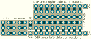
Front-panel DPDT switch: The “misc use area” in the picture to the upper right was designed to accept small 0.1" pin pitch DPDT board-mounted toggle switches. The front row of 3 pads accepts the mounting lugs, and the two groups of 6 behind it are for the 6 switch lugs and the hookup wires to run them to some other part of the circuit. The NKK G22AH switch, for example, sits with its mounting surface close to the front edge of the board when mounted here, so you could use it with the Serpac H-65 case. Or, the E-Switch 200 series M6 model has a mounting surface farther out, close to where the ALPS RK27’s mounting surface is, good for use in a larger case. These are just two examples out of many possibles. I found many other switches that will work here when designing this feature. A few more examples, only: Tyco TT21NGRA7T21/4. a few C&K GT22 variants...
Some ideas for what to do with the switch once you have it:
- bass boost
- power switch
- short the input cap
- alternate gain setting
- crossfeed setting, for a Modified Linkwitz Crossfeed, or...
Mini crossfeed: You could stuff a simple crossfeed circuit into the scratchpad, with a single DPDT switch (board-mounted or panel-mounted) for either on/off or high/low settings. You could combine this with the op-amp ideas above, using a circuit like the Meier crossfeed that requires buffering: run the wires from the amp’s input jacks to a dual-channel op-amp chip, with the channels configured as buffers to drive the crossfeed, which outputs to the PIMETA’s INPUTS connector.
Output jack connector: The Ox pads aren’t all clustered together, for layout reasons. If you wanted to fix that, say so you could connect the output jack to the board via a Molex KK connector, so you could easily disconnect the front panel from the board, you could do so easily in the scratchpad area. Pick any adjacent set of three 2-hole groups, and use one set of 3 holes for the connector, and the other three for the hookup wires back to each Ox pad. This is shown above.
Bass Boost
One of the most popular features of the PPA is its bass boost circuit. The cool thing about it is that it uses the op-amp circuit that already had to be there and it’s completely bypassable. As audio filters go, it’s about as problem-free as you could hope for.
There are a couple of ways to get bass boost with the PIMETA v2.
The first way is hinted at on the schematic. There are two extra pads off the ends of the thru-hole footprint for R4, plus the SMT pads on the bottom side. This allows for up to 3 components here, a resistor, a cap, and a switch. This is enough to give us a weaker form of bass boost than in the PPA, which I call “unity boost.” The difference is, the resulting amp is effectively just a unity-gain headphone driver with bass boost. This is fine for many situations. Most sources these days have enough voltage to drive headphones; they’re just current starved and have too high an output impedance to drive high-quality headphones to their full potential. A PIMETA in unity gain solves that problem. If you do this, I recommend using the outer pair of holes for the caps, the inner pair for the switch, and the 1206 SMT pads on the bottom side for the R4 resistor.
If you really do need voltage gain, you can still get a PPA-style bass boost. The thing you need, which we didn’t have room for on the PIMETA v2 board, is what the PPA calls R7: a resistor in series between the buffer output and R4. You can do this by running two pairs of hookup wires from the ends of R4R and R4L to the scratchpad area, then build out the bass boost circuit there. The needed changes will be obvious with a little study of the PPA schematic. Alternately, you can build this R7+R4+cap+switch circuit on a small chunk of perfboard and mount it vertically, like an add-on card in a PC, in the R4 thru-hole pads.
Stacking Buffers
Unlike with the PIMETA v1, I don’t recommend stacking the buffers in this design. Not only is it much more difficult with SO-8 chips than with the DIP-8 buffers used in v1, it’s less valuable, as the buffers in v2 are much more powerful. If you leave out the R11s, they can put out up to 700 mA for short periods, about what a stack of four buffers could manage in the preceding designs. A listening test should confirm that single buffers sound at least as good as a stack of the older buffers.
Leaving the Buffers Out
The buffers in the PIMETA design improve the sound of almost all op-amps when driving headphones, but there are several good reasons to leave the buffers out:
You might be using op-amps capable of driving headphones well all by themselves, like the OPA551, or AD8397.
You might be using the board as a preamp, not a headphone amp, and so don’t need the extra drive current
You might care more about saving money or power than getting the best possible sound. For instance, you might be using batteries most of the time, and need long run time.
You might not be able to find the buffers, or might be building a simpler amp first, with the intention of adding the buffers later.
Whatever the case, it’s easy to jumper the buffer positions in the PIMETA v2 board layout.
If you study the circuit board layout, you’ll see that there are two output pads per channel, with the label centered between them. The smaller of the two pads is intended for use with a jumper, the other leg of which goes in the R7 pad that connects to the op-amp. I recommend using resistor lead clippings for this.
You should also leave out the R6es, C6G, and jumper R5.
NiMH Battery Trickle Charger
IC1 and RCCS form a constant current source configured to take power from a wall power supply attached to the WALL connector and drive that trickle of current into nickel-chemistry (NiMH or NiCd) rechargeable batteries connected to BATT.
This is called a trickle, or “slow,” charger. A fast charger is hard on the batteries, and can easily damage them, so you have to have a lot of circuitry to prevent problems. This simple little circuit has none of that, so it can only safely charge the battery at a C/10 rate or slower. For instance, if you are using an 800 mAh AAA battery pack, you can drive up to 80 mA into it safely for long periods, theoretically getting a full charge from empty in 10 hours, though 12 is more realistic. When slow charging is acceptable, we can use simple circuits like this, and the batteries will last through more charge cycles than if you had used a fast charger.
Such long charging times make it quite possible that you will forget to unplug the amp as soon as it’s charged, but that’s okay, to a point. Modern NiMH batteries are made to tolerate some excessive trickle charging. The datasheets I’ve seen say you can trickle charge a NiMH battery for up to 30 days, but I’d be wary of doing so for more than a few days. Generally, I find plugging such things in overnight to be the best plan. Since NiMH batteries have no memory effect, you can safely use a partial charge, say 9 hours if you plug it in just before bed and unplug it to take it to work. If you don’t fully run it down during the day, 9 hours may be all you actually need to bring it back to full charge anyway.
This circuit is easy to configure:
Install D1 and D2. They keep the WALL and BATT power sources from interfering with each other, and ensure the batteries are cut off from the amp circuit while they charge.
Pick the value of RCCS so that you don’t exceed the maximum C/10 trickle charging current. To do this, take your battery’s amp-hour rating, divide by 10, and plug that in for I into the formula RCCS = 1.25 ÷ I. Taking that 800 mAh example above again, RCCS should be about 15 Ω. (A tenth of the amp-hour rating is 80 mA, or 0.08 A.) You should also calculate the power dissipated in the resistor to be sure you pick one that’s big enough to take it: P = 1.56 ÷ RCCS, or about a tenth of a watt in our example here, so an 1/8 W resistor would be just barely acceptable, and a 1/4 W resistor nice and safe.
-
Work out the proper charging voltage. A good rule of thumb is 1.5× the number of cells.
The best way to work out the perfect charging voltage is with an adjustable bench supply. Set the voltage to the smallest value that could possibly work for your pack, then increase it until the current meter stops changing. As the battery charges, the current measurement will dip, so tweak the voltage up a bit until it stabilizes. At the end of the charge cycle, you’ll have found the smallest voltage that does the job.
As long as you don’t exceed the limits of the LM317, you can’t use “too much” voltage here, so if in doubt, go a little higher. Any excess voltage will be dropped across the LM317, making it a little warmer than it has to be, but it’s not a big deal in a properly-configured trickler charger. An LM317 can drop 37 V without damage. Just remember, P = I2V, so if you make it drop 16 V at 0.25 A, it’s going to throw off 1 W of power as heat. With a TO-220 packaged LM317, you multiply watts dissipated by 50 to get temperature rise in °C without a heat sink, which tells us that even if we can keep most of the air inside our case at room temperature, the LM317 is going to be cooking at about 75°C with such a big drop across it! And without vents in the case, there’s no way it will be even that cool. Instead of adding a heat sink, much better to lower the voltage so it doesn’t have to turn so much voltage into heat. If we bring it down to a 5 V drop, we get only a 16°C rise over ambient, quite workable.
“9 V” rechargeables are tricky because there are three common configurations, with 6, 7, and 8 cells. Battery makers usually don’t tell you how many cells there are, but they do usually give the nominal voltage. Simply divide 1.2 V into that to get the cell count. 6-cell NiMHs are nominally 7.2 V, for instance. Incidentally, this is why 7.2 V batteries tend to have higher mAh ratings than 9.6 V batteries: they trade voltage for cell size.
A few more examples:
9 V 6-cell battery, rated at 250 mAh. C/10 is 25 mA, so RCCS can be as low as 50 Ω, and can be almost any old resistor because dissipation is only 31 mW. Minimum charging voltage will be around 9 V.
Eight 2100 mAh AA cells. C/10 is 210 mA, so RCCS can be as low as about 6 Ω. Let’s say we pick a more common 7.5 Ω resistor instead, because we can’t find such an odd value. Charging is a bit slower, being about 12.6 hours in the ideal case, probably more like 14 in real life, but we decide that’s okay. Power dissipation in RCCS isn’t much under 1/4 W, so to be safe we will want to use a 1/2 W RCCS here. Charging voltage should be at least 12 V. We might choose a 15 V power supply to be safe without a risk of too much heat dissipated in the LM317.
This circuit is only suitable for nickel-chemistry rechargeables. In particular, do not use it for lithium chemistries. They require a very different charging scheme. Lithiums are inherently more dangerous than nickel chemsistry batteries. They’re fairly easy to set on fire or make explode violently by mistreating them. This is why I decided to stick with NiMH for this feature. NiMH isn’t foolproof, but usually the worst that happens when you mistreat them is that they leak a bit.
Voltage Regulator Hack
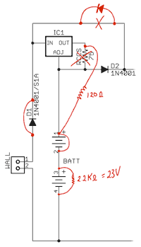
IC1, as you learned above, is for trickle-charging NiMH batteries. Some have wondered if you can use this LM317 for its intended purpose, as a voltage regulator to avoid having to have some sort of regulated power supply. Indeed, it is possible, as shown in the schematic at right.
I show this grotesque bit of hackery to discourage further thought on the matter. Far better to use an off-board regulated power supply. This avoids the need to modify the PIMETA board, and requires only two wires to the PIMETA board.
Optimizing the Loops in a Multiloop-Topology Amplifier
If you want to adjust the default multiloop resistor values, you should first read Walt Jung’s article Op-Amp Audio - Minimizing Input Errors.
The outer loop’s resistor values should be lower than the inner loop’s values. As a rough rule of thumb, make R3 five to ten times lower than R5. Also, remember that the lower these resistor values are, the more current your amp will use. I personally try to make R3 no lower than about 220 Ω, which means that R4 would be 2 kΩ for a gain of 10; then, R5 would be 1.2 kΩ or higher, making R6 120 kΩ for a ~100× inner loop gain. At the same time, you don’t want to go too high with these values, either, because that increases the chances that noise will get amplified along with the music signal. Avoid resistances over 1 MΩ if you can. Not only do larger values risk noise pickup in the amp, large-value 1% resistors tend to be expensive.
Biasing the Op-Amps into Class A
“Class A” refers to configuring an amplifier so that its output devices remain turned on all the time. This reduces thermal variation and eliminates crossover distortion, which makes the amp sound better.
The PIMETA v2 uses a somewhat novel circuit for this. LED1, RLED, Q1, and RBIAS + RBLIM form a typical sort of adjustable bipolar transistor constant current source. Q2 mirrors this sourced current twice and flips it, creating dual current sink paths through Q3L and Q3R to the V- rail. These sinks are connected to the OPALR outputs. In almost all op-amps, the output pin is connected to two bipolar transistors, one NPN, which usually performs better than its mate, a PNP. By sinking to the V- rail instead using current sources from the V+ rail, we get class A by turning on the NPNs, rather than the inferior PNPs.
One cool thing about this circuit is that it’s not only adjustable, but that one trim pot controls both sinks, biasing both op-amps in OPALR equally. You can therefore simply twiddle this pot while listening to judge the effect of changing how deep the op-amp outputs are pushed into class A. Different op-amps will require a different amount of current to sound their best. This design makes it easy to find the best balance between sound quality and power draw.
This circuit isn’t perfect. With the configuration described above, we use three times the class A biasing current, even though we’re only biasing two amp channels. This is because we have a “waste” path through Q2; its only purpose in the standard configuration is to set the current that gets mirrored to the sinks.
While designing this, I was irritated by this until I realized that people typically bias op-amps into class A with between 1 and 5 mA, exactly the current range people use for power LEDs. This explains the presence of LED2. When power efficiency is a concern, you can replace LED1 with a string of two or three silicon diodes, raise RLED by quite a lot (10× is about the limit) but still get a power indicator by dual-purposing the Q2 path current, running it through LED2. There’s no free lunch, of course. The first consequence of this is that the current source gets a bit “squishier” as silicon diodes make a poorer voltage reference for the CCS than an LED. The second is that sticking an LED in the Q2 path means the dropout voltage of the whole circuit goes up, though probably not enough to matter in a practical amp. It would matter if you were trying to run your PIMETA from a really low supply voltage, down in the 5 V range.
If you’re using LEDs to illuminate the interior of your amp, perhaps because it’s in a transparent or translucent enclosure, this feature has a side benefit, in that it gives you two LEDs to use. You’ve been able to do this since the original META42, but a single LED doesn’t put out a whole lot of light, when it comes to illumination. Keep in mind, though, the two LEDs have different current limiting schemes, which can cause them to have different brightnesses. LED1’s current is limited by RLED, so if you build your amp in the obvious way and use a resistor here, the LED will dim in a battery-powered PIMETA as the battery runs down, falling in voltage. This isn’t normally a problem, but if you also have LED in there, its brightness will stay constant because it’s in the CCS path, thus showing up the variability in the LED1 path. If you want to fix this, you can use a CRD in place of RLED, keeping the current in that path constant, too; there are CRDs available in the DO-35 package, making them easy substitutes for a resistor. The only unfortunate thing about that is that CRDs are expensive and not nearly as widely available as resistors and transistors.
The easiest way to adjust RBIAS is to first decide what bias current value you’re trying to achieve, then multiply that current by the value of RBLIM, giving the DC voltage drop across RBLIM when the current through it is what you want:
VRBLIM = Ibias × RBLIM
You can then put your meter’s probes across RBLIM, holding them in place with one hand like chopsticks while you adjust RBIAS with a small screwdriver in the other hand. When the meter gives the calculated DC voltage measurement, you know the bias current is set properly.
WARNING: If your probes slip while you’re adjusting the bias, they could short something else out as they jump around the board. Many parts of the PIMETA v2 circuit are tolerant of short circuits, but I won’t say there is no way to damage the amp by randomly shorting things together. If you are at all unsure of your ability to keep the probes on RBLIM, you can break the adjustment sequence up into parts: measure across RBLIM with a probe in each hand, set the probes aside, adjust RBIAS, measure again. It will take longer this way, but you will be able to keep the probes under control.
The “chopsticks method” is easiest to do when RBIAS is a surface-mount resistor, leaving the thru-holes open as sockets for the meter probes. If you’re using a thru-hole resistor, you want to use a meter with sharp tips so they dig into the solder joints a bit. Without either bit of stability, you should break the adjustment sequence up into parts, as recommended above.
Let’s work a practical example. Say you want 1 mA of bias (Ibias), and are using the standard 1 kΩ RBLIM value. That comes out to 1 V for VRBLIM. (Convenient, no?) So, you want to adjust RBIAS until you measure 1.0 V across RBLIM. If you have a typical 3- or 4-½ digit meter, you could probably tweak RBLIM to give 1.000 V on the display, though that level of precision is almost certainly inaudible. Those of you lucky enough to have a higher precision meter shouln’t bother trying to fill the display with zeroes.
Let’s go again with some less convenient values. Say we want to hit 2 mA (Ibias) and we have a 332 Ω RBLIM. The voltage drop across RBLIM, VRBLIM, would thus be 0.664 V.
While adjusting this, you should find that current goes up as you turn the pot’s adjustment shaft clockwise, like turning up the volume on an amp. You can use this rule to play with the current level without trying to measure voltage at the same time, by rearranging the formula above. Ibias = VRBLIM ÷ RBLIM gives you the bias current given the RBIAS value and the current DC voltage drop across it.
There’s another way to adjust the class A bias, which gives a more direct result: with the op-amp removed from the circuit, measure current between V+ and either pin 1 or pin 7 on the op-amp.
The obvious first problem is that it requires that you be able to remove the op-amp easily and replace it after you have made your measurement. If you aren’t using an op-amp socket, I can’t recommend the method at all. If you have to desolder anything to do this test, it’s probably easier to do it the normal way instead.
The direct measurement method also poses some risk to the meter. If the bias circuit isn’t working possibly, it could briefly send enough current through the meter to blow its fuse, or damage something inside if it isn’t properly fused. As a result, it is probably best to use this method only as a secondary test, after you have convinced yourself that the biasing circuit works.
This space intentionally left blank. :)